全志A527高性能8核SoC芯片详细规格参数datasheet |
您所在的位置:网站首页 › 芯片参数 › 全志A527高性能8核SoC芯片详细规格参数datasheet |
全志A527高性能8核SoC芯片详细规格参数datasheet
|
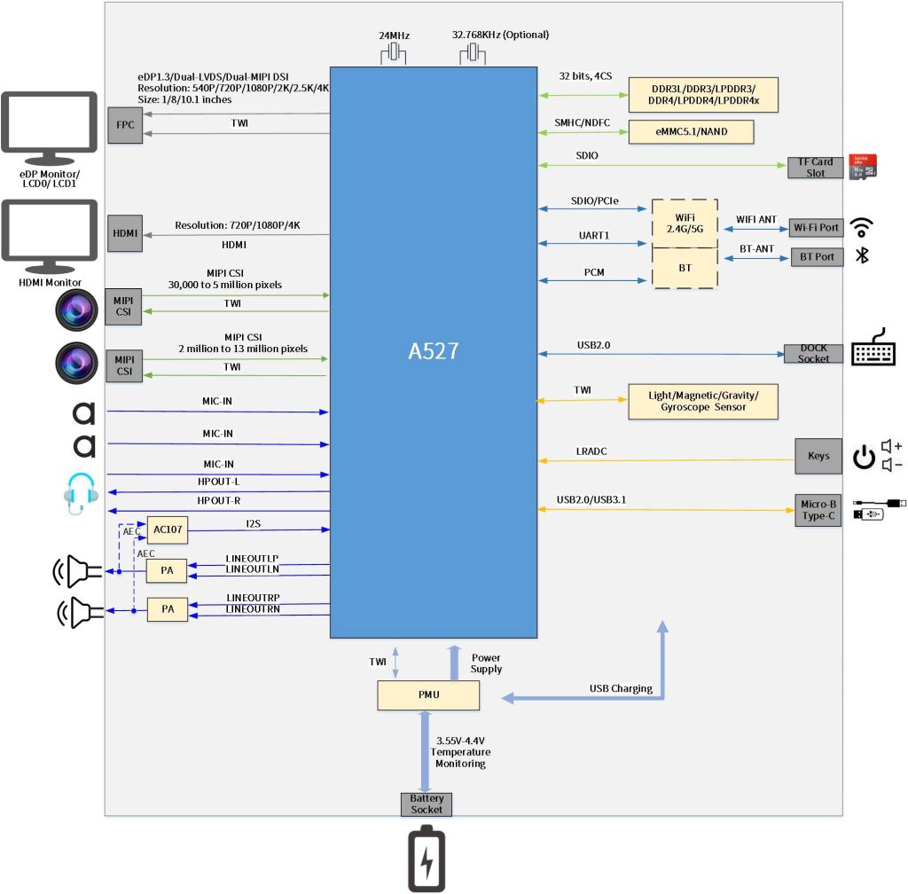
A527系列芯片是全志旗下的通用型八核SoC,可适用于ARM PC的高性能平台处理器,如二合一笔记本电脑、笔记本电脑、虚拟桌面和开源手持游戏机等。它集成了八核Cortex-A55、RISC-V CPU 和G57 MC01 GPU,以确保在线视频、网页浏览、3D游戏等日常应用的快速响应和平稳运行。A527系列还支持内存接口(DDR3/DDR3L/LPDDR3/DDR4/LPDDR4/LPDR4X、eMMC、NAND、SPI NAND)、高速接口(PCIe2.1和USB3.1)、多视频输出接口(2xRGB/2xDual LVDS/MIPI-DSI/eDP/HDMI)和视频输入接口(MIPI CSI)。此外,该芯片系列支持[email protected]解码器,[email protected]编码器、DI、SmartColor系统,为用户提供卓越的视频体验。A527系列可应用于GMS平板电脑、双屏收银机和大屏幕显示器市场。 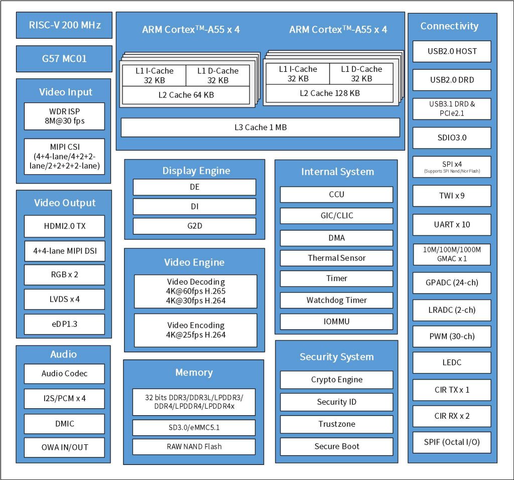 全志A527功能框图 3.1 CPU Architecture Octa-core ARM CortexTM-A55 in a DynamIQ big.LITTLE configuration – 32 KB L1 I-cache and 32 KB L1 D-cache per A55 core – Optional 64KB L2 cache per “LITTLE” core – Optional 128KB L2 cache per “big” core Single –core RISC-V, up to 200 MHz – 16 KB I-cache and 16 KB D-cache – RV32IMAFC instructions 3.2 GPU Architecture ARM G57 MC01 GPU Supports OpenGL ES 3.2/2.0/1.1, Vulkan1.1/1.2/1.3, and OpenCL2.2 Anti-aliasing algorithm High memory bandwidth and low power consumption in 3D graphics processing 3.3 Memory Subsystem 3.3.1 Boot ROM (BROM) On-chip memory Supports system boot from the following devices: – SD Card – eMMC – RAW NAND Flash – SPI NOR Flash (Quad Mode and Single Mode) – SPI NAND Flash Supports mandatory upgrade process through USB or SD card Supports GPADC0 pin and eFuse module to select the boot media type Supports normal booting and secure booting Secure BROM loads only certified firmware 3.3.2 RAW NAND Flash Up to 80-bit ECC per 1024 bytes Supports 1K/2K/4K/8K/16K/32K bytes page size Up to 8-bit data bus width Supports SLC/MLC/TLC flash and EF-NAND Supports SDR, ONFI DDR1.0, Toggle DDR1.0, ONFI DDR2.0, and Toggle DDR2.0 RAW NAND FLASH 3.3.3 SDRAM 32-bit DDR3/DDR3L/LPDDR3/DDR4/LPDDR4/LPDDR4X interface Memory capacity up to 4GB 4 chip select lines for LPDDR3, LPDDR4, and LPDDR4X (especially the 64-bit LPDDR3, LPDDR4,and LPDDR4X) Clock frequency up to 1066 MHz for DDR3, DDR3L, and LPDDR3 Clock frequency up to 1200 MHz for DDR4, LPDDR4, and LPDDR4x 3.3.4 SMHC Three SD/MMC host controller (SMHC) interfaces – SMHC0, compliant with the protocol Secure Digital Memory (SD3.0) – SMHC1, compliant with the protocol Secure Digital I/O (SDIO3.0) – SMHC2, compliant with the protocol Multimedia Card (eMMC5.1) The SMHC0 and the SMHC1 support the following: – 1-bit or 4-bit data width – Maximum performance: SDR mode 200 [email protected] V IO pad DDR mode 50 [email protected] V IO pad SDR mode 50 [email protected] V IO pad The SMHC2 supports the following: – 1-bit, 4-bit, or 8-bit data width – Supports HS400 mode and HS200 mode – Maximum performance SDR mode [email protected] IO pad DDR mode [email protected] IO pad SDR mode [email protected] IO pad DDR mode [email protected] IO pad Support block size of 1 to 65535 bytes Support hardware CRC generation and error detection 3.4 Video and Graphics 3.4.1 Display Engine (DE) Output size up to 4096 x 2048 Supports seven alpha blending channels for main display and two display outputs Supports four overlay layers in each channel, and has an independent scaler Supports potter-duff compatible blending operation Supports AFBC buffer decoder Supports vertical keystone correction Input format – Semi-planar of YUV422/YUV420/YUV411/P010/P210 – Planar of YUV422/YUV420/ YUV411 – ARGB8888/XRGB8888/RGB888/ARGB4444/ ARGB1555/RGB565 Output format: 8-bit or 10-bit YUV444/YUV422/YUV420/RGB444 Frame Packing/Top-and-Bottom/Side-by-Side Full/Side-by-Side Half 3D format data 10-bit processing path for HDR video SmartColor5.0 for excellent display experience – Adaptive de-noising for compression noise or mosquito noise with yuv420/422 input – Adaptive super resolution scaler – Adaptive local dynamic contrast enhancement – Adaptive detail/edge enhancement – Adaptive color enhancement (blue-stretch, green-stretch, and fresh tone correction) and skin tone protection – Hue gain, saturation gain, and value gain controller – Fully programmable color matrix – Dynamic gamma Supports write back for high efficient dual display and miracast Supports register configuration queue for register update function 3.4.2 De-interlacer (DI) Only off-line processing mode Video resolution from 32×32 to 2048×1280 pixel Input data format: 8-bit NV12/NV21/YV12 and planar YUV422/planar YUV422 UV-combined Output data format – 8-bit NV12/NV21/YV12 and planar YUV422/planar YUV422 UV-combined for DIT – YV12/planar YUV422 for TNR Weave/pixel-motion-adaptive de-interlace method Temporal noise reduction Film mode detection with video-on-film detection Performance – Module clock 120MHz for 1080P@60Hz YUV420 with all functions enable – Module clock 150MHz for 1080P@60Hz YUV422 with all functions enable 3.4.3 Graphic 2D (G2D) Layer size up to 2048×2048 pixels Input format and output format contain the following: – YUV422 (semi-planar and planar format) – YUV420 (semi-planar and planar format) – P010, P210, P410, and Y8 – ARGB8888, XRGB8888, RGB888, ARGB4444, ARGB1555, ARGB2101010, and RGB565 Multiple rotation types – Horizontal flip and vertical flip – 0, 90, 180, or 270 degrees’ rotation in clockwise direction 3.4.4 Video Engine 3.4.4.1 Video Decoding Supports ITU-T H.265 Main/Main10, level 6.1 – Maximum video resolution:8192×4320 – Maximum decoding rate: 3840×2160@60fps or 3840×2160@30fps, 10 bits Supports VP9 Profile0/ Profile2, level 6.1 – Maximum video resolution: 8192 x 4320 – Maximum decoding rate: 3840mx2160@60fps or 3840×2160@30fps, 10 bits Supports ITU-T H.264 Base/Main/High Profile@Level 4.2 – Maximum video resolution: 3840 x 2160 – Maximum decoding rate: 3840×2160@30fps, 8 bits 3.4.4.2 Video Encoding H.264 BP/MP/HP encoding – Supports 4K@25fps@8bits – Maximum resolution: 4096 x 4096 (16 megapixels) – Supports I/P frame type – Supports CBR, VBR and FIXEDQP modes – Supports region of interest(ROI) encoding, a maximum of eight ROIs JPEG baseline encoding – MJPEG encoder supports 4K@15fps – JPEG encoder supports YUV420, YUV422 and YUV444 format 3.5 Video Output 3.5.1 eDP1.3 Up to 2.5K@60fps and 4K@30fps 1-lane, 2-lane, or 4-lane transmission, up to 2.7 Gbit/s per lane Video formats: RGB, YCbCr4:4:4, and YCbCr4:2:2 Color depth: 8-bit and 10-bit per channel Supports I2S interface – Supports mono sound, stereo sound, and 7.1 surround sound – Maximum sampling rate: 192 KHz Full link training Hot plug detection AUX channel – Maximum working frequency: 1MHz – Adopts Manchester-II encoding Clock spread spectrum Programmable voltage swing and pre-emphasis Embedded ESD 3.5.2 MIPI DSI Compliance with MIPI DSI V1.02 Up to 1.5 Gbit/s for each lane Supports 4-lane MIPI DSI, up to 1280 x 720@60fps and 1920 x 1200@60fps Supports 4+4-lane MIPI DSI, up to 2560 x 1600@60fps, 3840×2160@45fps, and 4096 x 2160@45fps Supports non-burst mode with sync pulse/sync event and burst mode Pixel format: RGB888, RGB666, RGB666 loosely packed and RGB565 Supports continuous and non-continuous lane clock modes Generic commands support bidirectional communication in LP through data lane 0 Supports low power data transmission Supports ULPS and escape modes Supports hardware checksum 3.5.3 TCON LCD Three TCON LCD controllers: TCON_LCD0, TCON_LCD1, and TCON_LCD2. TCON_LCD0 supports the following: – Supports RGB interface with DE/SYNC mode, up to 1920 x 1080@60fps – Supports serial RGB/dummy RGB interface, up to 800 x 480@60fps – Supports LVDS interface with dual link, up to 1920 x 1080@60fps – Supports LVDS interface with single link, up to 1366 x 768@60fps – Dither function for RGB888, RGB666, and RGB565 – Supports i8080 interface, up to 800 x 480@60fps – Supports BT656 interface for NTSC and PAL – Supports MIPI DSI interface with dual link, up to 2560×1600@60fps, 3840×2160@45fps and 4096×2160@45fps – Supports MIPI DSI interface with single link, up to 1920×1200@60fps TCON_LCD1 supports MIPI DSI interface with single link, up to 1920×1200@60fps TCON_LCD2 supports the following: – Supports RGB interface with DE/SYNC mode, up to 1280×720@60fps – Supports serial RGB/dummy RGB interface, up to 800×480@60fps – Supports LVDS interface with dual link, up to 1920×1080@60fps – Supports LVDS interface with single link, up to 1366×768@60fps – Supports i8080 interface, up to 800×480@60fps – Supports BT656 interface for NTSC and PAL – Dither function for RGB888, RGB666, and RGB565 3.5.4 TCON TV Two TCON TV controllers: TCON_TV0 for HDMI 2.0b and TCON_TV1 for eDP1.3 Up to 4K@60Hz Output format: – 8-bit or 10-bit pixel depth – HV 3.5.5 HDMI One HDMI2.0 TX interface, supporting HDCP1.4 Supports 3840×2160, 1920×1080, and 1280×720 resolution Up to 4K@60fps for 2D display and up to 4K@30fps for 3D display Supports several data formats including RGB888, YUV444, YUV422, and YUV420 Supports I2S, 192 kHz sampling rate, 8 sound channels Supports up to 3840×2160@60 10bit input, 3 Data lanes, 6 Gbit/s per lane for YUV422 Supports DDC/CEC, 5 V tolerant voltage 3.6 Video Input 3.6.1 ISP Supports one individual image signal processor(ISP), with maximum resolution of 3264×4224 in online mode Maximum frame rate of 8M@30fps 2F-WDR Supports off-line mode Supports WDR spilt, 2F-WDR line-based stitch, dynamic range compression (DRC), tone mapping, digital gain, gamma correction, defect pixel correction (DPC), cross talk correction (CTC), and chromatic aberration correction (CAC) Supports 2D/3D noise reduction, bayer interpolation, sharpen, white balance, and color enhancement Adjustable 3A functions: automatic white balance (AWB), automatic exposure (AE), and automatic focus (AF) Supports anti-flick detection statistics, and histogram statistics 3.6.2 VIPP Four VIPP YUV422 or YUV420 outputs Maximum resolution of 3264×4224 Each VIPP has one sub-VIPP in online mode Each VIPP has maximum four sub-VIPPs for time division multiplexing in offline mode Each Sub-VIPP supports the following: – Crop – 1 to 1/16 scaling for height and width – 16 ORLs Supports graphics mirror and flip 3.6.3 MIPI CSI 8M@30fps RAW12 2F-WDR, size up to 3264(H) x 2448(V) 4+4-lane, 4+2+2-lane, or 2+2+2+2-lane MIPI Interface – MIPI CSI2 V1.1 – MIPI DPHY V1.1 – 2.0 Gbit/s per lane Crop function Frame-rate decreasing via software 4 DMA controllers for 4 video stream storage – Conversion of interlaced input to progressive output (anti-aliasing and noise reduction are not supported) – Data conversion supports: YUV422 to YUV420, YUV422 to YUV400, YUV420 to YUV400 – Horizontal and vertical flip 3.6.4 Parallel CSI 16-bit digital camera interface Supports 8/10/12/16-bit width Supports BT.656, BT.601, BT.1120 interface Dual Data Rate (DDR) sample mode with pixel clock up to 148.5MHz Supports ITU-R BT.656 up to 4*720P@30fps Supports ITU-R BT.1120 up to 4*1080P@30fps 3.7 System Peripherals 3.7.1 Clock Controller Unit (CCU) 11 PLLs One on-chip RC oscillator Supports one external 24 MHz DCXO and one external 32.768 kHz oscillator Supports clock configuration and clock generation for corresponding modules Supports software-controlled clock gating and software-controlled reset for corresponding modules 3.7.2 DMAC Two 16-ch DMAs Provides 53 peripheral DMA requests for data reading and 53 peripheral DMA requests for data writing Transferring data with linked list Flexible data width: 8 bits, 16 bits, or 32 bits Programmable DMA burst length DRQ response includes waiting mode and handshake mode Supports non-aligned transform for memory devices DMA channels that support the following: – Pausing DMA – BMODE and I/O speed mode – DMA timeout 3.7.3 I/O Memory Management Unit (IOMMU) Supports virtual address to physical address mapping by hardware implementation Supports ISP, CSI, VE_MBUS0, VE_MBUS1, G2D, DE, and DI parallel address mapping Supports ISP, CSI, VE_MBUS0, VE_MBUS1, G2D, DE, and DI bypass function independently Supports ISP, CSI, VE_MBUS0, VE_MBUS1, G2D, DE, and DI pre-fetch independently Supports ISP, CSI, VE_MBUS0, VE_MBUS1, G2D, DE, and DI interrupt handing mechanism independently Supports 2 levels TLB (level1 TLB for special using, and level2 TLB for sharing) Supports TLB Fully cleared and Partially disabled Supports trigger PTW behavior when TLB miss Supports checking the permission 3.7.4 Message Box (MSGBOX) Supports communication between two CPUs through one way channels. Each CPU has one MSGBOX and can only read or write in one communication – CPUX_MSGBOX: CPUS/RISC-V write; ARM CPU read – CPUS_MSGBOX: ARM CPU/RISC-V write; CPUS read – RISCV_MSGBOX: ARM CPU/CPUS write; RISC-V read The channel between two CPU has 4 channels, and the FIFO depth of a channel is 8 x 32 bits Supports interrupts 3.7.5 Power Reset Clock Management (PRCM) Two PRCMs: STBY_PRCM and MCU_PRCM 1 PLL CPUS Clock Configuration APBS Clock Configuration CPUS Module Clock Configuration CPUS Module BUS Gating and Reset RAM configure Control for STBY_PRCM 3.7.6 RTC Provides a 16-bit counter for counting day, 5-bit counter for counting hour, 6-bit counter for counting minute, 6-bit counter for counting second External connect a 32.768 kHz low-frequency oscillator for count clock Timer frequency is 1 kHz Configurable initial value by software anytime Supports fanout function of internal 32K clock Supports timing alarm, and generates interrupt and wakeup the external devices 8 general purpose registers for storing power-off information in AON domain 3.7.7 Spinlock Supports 32 lock units Two kinds of lock status: locked and unlocked Lock time of the processor is predictable (less than 200 cycles) 3.7.8 Thermal Sensor Controller (THS) Two THS controllers – THS0, including TSENSOR4 – THS1, including TSENSOR0, TSENSOR1, TSENSOR2 Temperature accuracy: ±5°C from -40°C to +60°C, ±3°C from +60°C to +125°C Averaging filter for thermal sensor reading Supports over-temperature protection interrupt and over-temperature alarm interrupt 3.7.9 Timer Configurable counting clock: 32KHz, 24MHz, 16MHz, or 200MHz Programmable 56-bit down timer Two working modes: periodic mode and single count mode Generates an interrupt when the count is decreased to 0 3.7.10 Watchdog Timer (WDT) Supports 12 initial values Supports the generation of timeout interrupts Supports the generation of reset signals Supports Watchdog Restart 3.8 Audio Subsystem 3.8.1 Audio Codec Two audio digital-to-analog converter (DAC) channels – 16-bit and 20-bit sample resolution – 8 kHz to 192 kHz DAC sample rate – 100 ± 2 dB SNR@A-weight, -85 ± 3 dB THD+N Three audio outputs – One stereo headphone output: HPOUTL/R – Two differential lineout outputs: LINEOUTLP/N and LINEOUTRP/N Three audio analog-to-digital converter (ADC) channels – 16-bit and 20-bit sample resolution – 8 kHz to 48 kHz ADC sample rate – 95 ± 3 dB SNR@A-weight, -80 ± 3 dB THD+N Three differential microphone inputs: MICIN1P/1N, MICIN2P/2N, and MICIN3P/3N (for echo reduction) Two low-noise analog microphone bias outputs: MBIAS and HBIAS Supports Dynamic Range Controller adjusting the DAC playback and ADC recording One 128×20-bits FIFO for DAC data transmit, one 128×20-bits FIFO for ADC data receive Programmable FIFO thresholds Supports interrupts and DMA Internal ALDO output for AVCC 3.8.2 I2S/PCM Four I2S/PCM external interfaces (I2S0, I2S1, I2S2, and I2S3) for connecting external power amplifier and MIC ADC Compliant with standard Philips Inter-IC sound (I2S) bus specification – Left-justified, Right-justified, PCM mode, and TDM format – Programmable PCM frame width: 1 BCLK width (short frame) and 2 BCLKs width (long frame) FIFOs for transmitting and receiving data – Programmable FIFO thresholds – 128 depth x 32-bit width TXFIFO and 64 depth x 32-bit width RXFIFO Supports multiple function clocks – Clock up to 24.576 MHz Data Output of I2S/PCM in Master mode (Only if the IO PAD and Peripheral I2S/PCM satisfy Timing Parameters) – Clock up to 12.288 MHz Data Input of I2S/PCM in Master mode Supports TX/RX DMA slave interface Supports multiple application scenarios – Up to 16 channels (fs = 48 kHz) which has adjustable width from 8-bit to 32-bit – Sample rate from 8 kHz to 384 kHz (sample rate * channel * slot width ≤ 24.576 MHz) – 8-bit u-law and 8-bit A-law companded sample Supports master/slave mode 3.8.3 DMIC Supports maximum 8 digital PDM microphones Supports sample rate from 8 kHz to 48 kHz 3.8.4 One Wire Audio (OWA) One OWA TX and One OWA RX Compliance with S/PDIF interface IEC-60958 and IEC-61937 transmitter and receiver functionality IEC-60958 supports data formats: 16 bits, 20 bits, and 24 bits TXFIFO and RXFIFO – One 128×24bits TXFIFO and one 64×24bits RXFIFO for audio data transfer – Programmable FIFO thresholds Supports TX/RX DMA slave interface Multiple function clock – Separate clock for OWA TX and OWA RX – The clock of TX function includes 24.576 MHz and 22.5792 MHz – The clock of RX function includes 24.576*8 MHz Supports hardware parity on TX/RX – Hardware parity generation on the transmitter – Hardware parity checking on the receiver Supports channel status capture on the receiver Supports channel sample rate capture on the receiver Supports insertion detection for the receiver Supports channel status insertion for the transmitter 3.9 Security System 3.9.1 Crypto Engine (CE) Symmetrical algorithm: – AES symmetrical algorithm Key size: 128/192/256 bits CFB mode includes: CFB1, CFB8, CFB64, and CFB128 CTR mode includes: CTR16, CTR32, CTR64, and CTR128 Supports ECB, CBC, CTS, OFB, CBC-MAC, and GCM modes – DES symmetrical algorithm CTR mode, includes: CTR16, CTR32, and CTR64 Supports ECB, CBC, and CBC-MAC mode – Supports 3DES – SM4 symmetrical algorithm supports ECB and CBC mode Hash algorithms – Support MD5, SHA1, SHA224, SHA256, SHA384, SHA512, and SM3 – Support HMAC-SHA1, HMAC-SHA256 Random bit generator algorithms – Support PRNG, 175 bits seed width, and output with multiple of 5 words – Support TRNG, post-process by hardware with SHA256, output with multiple of 8 words Public key algorithms – Support RSA public key algorithms: 512/1024/2048/3072/4096-bit width – Support ECC public key algorithms: 160/224/256/384/521-bit width – Support SM2 algorithms 3.9.2 Security ID (SID) 4 Kbits eFuse Supports secure and non-secure world in eFuse The register configuration of SID is always in non-secure world Backup eFuse information by using SID_SRAM One-time programming Selecting double-bit check by parameter definition Data scrambling Reading and writing protection 3.9.3 Secure Memory Control (SMC) The SMC is always secure, only secure CPUX can access the SMC Sets secure area of DRAM Supports Master and address protection Sets secure property that Master accesses to DRAM Sets DRM area Maximum 16 regions and Master has access to each region 3.9.4 Secure Peripherals Control (SPC) The SPC is always secure, only secure CPU can access the SPC Sets secure property of peripherals 3.10 External Peripherals 3.10.1 CIR Receiver (CIR_RX) Two CIR_RX interfaces Full physical layer implementation Supports NEC format infra data Supports CIR for remote control 64×8 bits FIFO for data buffer Sample clock up to 1 MHz 3.10.2 CIR Transmitter (CIR_TX) One CIR_TX interface Full physical layer implementation Arbitrary wave generator Configurable carrier frequency Handshake mode and waiting mode of DMA 128 bytes FIFO for data buffer Supports Interrupts and DMA 3.10.3 GMAC One GMAC interface (GMAC1) for connecting to external Ethernet PHY Compliant with the IEEE 802.3-2015 standard Supports 10/100/1000 Mbit/s data transfer rates Supports RMII/RGMII PHY interface AMBA4 AXI master interface with 64bit data transfer Supports both full-duplex and half-duplex operation Full-duplex flow control IEEE 1588-2008 for precision networked clock synchronization, support Ethernet packet timestamping as described in IEEE 1588-2002 and IEEE 1588-2008 Programmable frame length to support Standard or Jumbo Ethernet frames with sizes up to 16 KB Source Address field and VLAN insertion or replacement, Double VLAN Transmit TCP/IP Checksum Offload Supports a variety of flexible address filtering modes(include Hash filter function) Optimization for packet-oriented DMA transfers with frame delimiters – Supports linked-list descriptor list structure – Descriptor architecture, allowing large blocks of data transfer with minimum CPU intervention: each descriptor can transfer up to 32 KB of data – Comprehensive status reporting for normal operation and transfers with errors Supports 4KB TXFIFO for transmission packets and 8KB RXFIFO for reception packets Supports 16 Descriptors Descriptor Pre-fetch cache for TXDMA and RX DMA Programmable interrupt options for different operational conditions Supports MDIO Interface for PHY device configuration and management Configurable big-endian and little-endian mode for Transmit and Receive paths Supports statistics on the received and transmitted packets Supports split header 3.10.4 General Purpose ADC (GPADC) 24-ch SAR ADC 64 FIFO depth of data register 12-bit sampling resolution and 10-bit precision Power reference voltage: VCC-ADC, analog input voltage range: 0 to 1.8V Maximum sampling frequency up to 1 MHz Supports three operation modes: single conversion mode, continuous conversion mode,burst conversion mode 3.10.5 LEDC Configurable LED output high/low level width Configurable LED reset time LEDC data supports DMA configuration mode and CPU configuration mode Maximum 1024 LEDs serial connect Configurable interval time between data packets and frame data Configurable RGB display mode 3.10.6 Low Rate ADC (LRADC) 2-ch LRADC input 6-bit resolution Sampling rate up to 2 kHz Supports hold key and general key Supports normal, continue and single work mode Power supply voltage:1.8V, power reference voltage:1.35V 3.10.7 USB2.0 DRD One USB2.0 DRD (USB0), with integrated USB 2.0 analog PHY Complies with USB2.0 Specification Supports static host operation: – Compatible with Enhanced Host Controller Interface (EHCI) Specification, Version 1.0 – Compatible with Open Host Controller Interface (OHCI) Specification, Version 1.0a – Supports High-Speed (HS, 480 Mbit/s), Full-Speed (FS, 12 Mbit/s), and Low-Speed (LS, 1.5 Mbit/s) – Supports only 1 USB Root port shared between EHCI and OHCI Supports static device operation: – Supports High-Speed (HS, 480 Mbit/s), Full-Speed (FS, 12 Mbit/s) – Supports bi-directional endpoint0 (EP0) for Control transfer – Up to 10 user-configurable endpoints (EP1 IN/OUT, EP2 IN/OUT, EP3 IN/OUT, EP4 IN/OUT, EP5 IN/OUT) for Bulk transfer, Isochronous transfer and Interrupt transfer – Up to (8 KB + 64 Bytes) FIFO for all EPs (including EP0) – Supports interface to an external Normal DMA controller for every EP Supports an internal DMA controller for data transfer with memory Supports High-Bandwidth Isochronous & Interrupt transfers Automated splitting/combining of packets for Bulk transfers Includes automatic PING capabilities Soft connect/disconnect function Hardware handles all data transfer Power optimization and power management capabilities Device and host controller share an 8K SRAM and a physical PHY 3.10.8 USB2.0 HOST One USB 2.0 HOST (USB1), with integrated USB 2.0 analog PHY Supports High-Speed (HS, 480 Mbit/s), Full-Speed (FS, 12 Mbit/s) and Low-Speed (LS, 1.5 Mbit/s) Device Compatible with Enhanced Host Controller Interface (EHCI) Specification, Version 1.0 Compatible with Open Host Controller Interface (OHCI) Specification, Version 1.0a Supports only 1 USB Root port shared between EHCI and OHCI An internal DMA Controller for data transfer with memory Supports the UTMI+ Level 3 interface and 8-bit bidirectional data buses Industry-standard AMBA High-Performance Bus (AHB), fully compliant with the AMBA Specification, Revision 2.0. 32-bit Little Endian AMBA AHB Slave Bus for Register Access 32-bit Little Endian AMBA AHB Master Bus for Memory Access 3.10.9 PCIe2.1&USB3.1 System PCIe2.1&USB3.1 system contains 1 PCIe2.1&USB3.1 combo PHY, 1 PCIe2.1 controller and 1 USB3.1 GEN1 DRD controller. 3.10.9.1 PCIe2.1 Compliance to PCI Express Base Specification, Revision 2.1 Supports Gen1(2.5 Gbit/s), Gen2 (5.0 Gbit/s) speed Supports 62.5MHz/125 MHz operation on PIPE interface for Gen1/Gen2, respectively Constant 32-bit PIPE width for Gen1/Gen2 modes Supports Root Complex (RC) mode Supports 1 lane link width Eight Traffic Classes (TC) Maximum payload size of 1K bytes 8 inbound and 8 outbound address translation regions 4 write/read channels for embedded DMA Maximum number of non-posted outstanding transactions: 32 Supports Active State Power Management (ASPM) Supports Advanced Error Reporting (AER) Supports MSI interrupt 3.10.9.2 USB3.1 DRD NOTE USB2.0 PHY and USB3.1 PHY share the same controller. They cannot be used simultaneously. Compliant with USB3.1 GEN1 Specification One USB 2.0 UTMI+ PHY (USB2) One USB3.1 PIPE PHY (USB3) USB3.1 DRD Device mode supports the following: – Super-Speed (SS, 5 Gbit/s) for USB3.1 PHY – High-Speed (HS, 480 Mbit/s) and Full-Speed (FS, 12-Mbit/s) for USB2.0 PHY USB3.1 DRD HOST mode supports the following: – Super-Speed (SS, 5 Gbit/s) for USB3.1 PHY – High-Speed (HS, 480 Mbit/s), Full-Speed (FS, 12 Mbit/s) and Low-Speed (LS, 1.5 Mbit/s) for USB2.0 PHY Supports Device or Host operation at a time AXI interface for DMA operation Reading and writing access to Control and Status Registers (CSRs) through AHB Slave interface Up to 10 Endpoints, including control Endpoint 0 in Device mode: – 5 IN Endpoints: User EP1 IN, EP2 IN, EP3 IN, EP4 IN, Control EP0 IN – 5 OUT Endpoints: User EP1 OUT, EP2 OUT, EP3 OUT, EP4 OUT, Control EP0 OUT Simultaneous IN and OUT transfer in Super-Speed mode Dual-port interfaces for TX data buffering, RX data prefetching, descriptor caching, and register caching Three RAMs: Rx data FIFO RAM, TX data FIFO RAM, and descriptor/register Cache RAM Hardware handles all data transfer Implements both static and dynamic power reduction techniques at multiple levels 3.10.10 PWM Up to 20 PWM channels and 10 S-PWM channels Maximum 16 independent PWM channels for one PWM controller – Supports PWM continuous mode output – Supports PWM pulse mode output, and the pulse number is configurable – Output frequency range: 0 to 24 MHz (when the clock source is DCXO24M) 0 to 100 MHz (when the clock source is APB1 clock) – Various duty-cycle: 0% to 100% – Minimum resolution: 1/65536 Maximum 8 complementary pairs output for one PWM controller – The pairing methods are as follows. The components are PWM output signals. PWM Channels PWM0 + PWM1, PWM2 + PWM3, PWM4 + PWM5, PWM6 + PWM7, PWM8 + PWM9, PWM10 + PWM11, PWM12 + PWM13, PWM14 + PWM15, PWM16 + PWM17, PWM18 + PWM19 S-PWM Channels S-PWM0 + S-PWM1, S-PWM2 + S-PWM3, S-PWM4 + S-PWM5, S-PWM6 + S-PWM7, S-PWM8 + S-PWM9 – Supports dead-zone generator, and the dead-zone time is configurable Maximum 4 group of PWM channel output for controlling stepping motors – Supports any plural channels to form a group, and output the same duty-cycle pulse – In group mode, the relative phase of the output waveform for each channel is configurable Maximum 16 channels capture input – Supports rising edge detection and falling edge detection for input waveform pulse – Supports pulse-width measurement for input waveform pulse 3.10.11 SPI and SPI_DBI Up to 4 SPI controllers: SPI0, SPI2, and S_SPI0, supporting SPI mode SPI1, supporting SPI mode and display bus interface (DBI) mode SPI mode Multiple SPI modes: – Master mode and slave mode for standard SPI – Master mode for Dual-Output/Dual-Input SPI and Dual I/O SPI – Master mode for Quad-Output/Quad-Input SPI – Master mode for 3-wire SPI, with programmable serial data frame length of 1 bit to 32 bits Maximum clock frequency: 100MHz TX/RX DMA slave interface 8-bit wide by 64-entry FIFO for both transmitting and receiving data Supports mode0, mode1, mode2, and mode3 Polarity and phase of the Chip Select (SPI_SS) and SPI Clock (SPI_SCLK) are configurable DBI mode DBI Type C 3 Line/4 Line Interface Mode 2 Data Lane Interface Mode RGB111/444/565/666/888 video format Maximum resolution of RGB666 240 x 320@30Hz with single data lane Maximum resolution of RGB888 240 x 320@60Hz or 320 x 480@30Hz with dual data lane Tearing effect Software flexible control video frame rate 3.10.12 SPI Flash Controller (SPIFC) Supports multiple SPI modes – Standard SPI – Dual-Input/Dual-Output SPI and Dual-I/O SPI – Quad-Input/Quad-Output SPI, Quad-I/O SPI, and QPI – Octal-Input/Octal-Output SPI, Octal-I/O SPI, and OPI – 3-wire SPI with programmable serial data frame length of 1 bit to 32 bits Supports STR mode and DTR mode, and DTR mode supports DQS signal High Speed Clock Frequency – 150MHz for STR Mode – 100MHz for DTR Mode Software Write Protection – Write protection for all/portion of memory via software – Top/Bottom Block protection Programmable delay between transactions Support Mode0, Mode1, Mode2 and Mode3 Support control signal configuration – Up to four chip selects to support multiple peripherals – Polarity and phase of the Chip Select (SPI_SS) and SPI Clock (SPI_SCLK) are configurable 3.10.13 Two Wire Interface (TWI) Up to 9 TWI controllers – TWI0, TWI1, TWI2, TWI3, TWI4, and TWI5 – S_TWI0, S_TWI1, and S_TWI2 Compliant with I2C bus standard 7-bit and 10-bit device addressing modes Standard mode (up to 100 Kbit/s) and fast mode (up to 400 Kbit/s) Supports general call and start byte Master mode supports the following: – Bus arbitration in the case of multiple master devices – Clock synchronization and bit and byte waiting – Packet transmission and DMA Slave mode supports Interrupt on address detection 3.10.14 UART Up to 10 UART controllers – UART0, UART1, UART2, UART3, UART4, UART5, UART6, and UART7 – S_UART0 and S_UART1 Compatible with industry-standard 16450/16550 UARTs Two separate FIFOs: one is RX FIFO, and the other is TX FIFO – Each of them is 64 bytes for UART0, S_UART0, and S_UART1 – Each of them is 128 bytes for UART1, UART2, UART3, UART4, UART5, UART6, and UART7 The working reference clock is from the APB bus clock – Speed up to 10 Mbit/s with 160 MHz APB clock (excluding S_UART0 and S_UART1) – Speed up to 5 Mbit/s with 80 MHz APB clock (excluding S_UART0 and S_UART1) – Speed up to 3.75 Mbit/s with 60 MHz APB clock (excluding S_UART0 and S_UART1) – Speed up to 1.5 Mbit/s with 24 MHz APB clock 5 to 8 data bits for RS-232 format, or 9 bits RS-485 format 1, 1.5 or 2 stop bit (s) Programmable parity (even, odd, or no parity) Supports TX/RX DMA slave controller interface Supports software/hardware flow control Supports IrDA-compatible slow infrared (SIR) format Supports auto-flow by using CTS & RTS (excluding UART0, S_UART0, and S_UART1) 3.11 Package FCCSP 664balls, 17 mm x 17 mm size, 0.5 mm ball pitch, 0.3 mm ball size 全志A527应用框图:
|
 点击查看更多芯片的datasheet
【本文地址】
今日新闻 |
推荐新闻 |