|
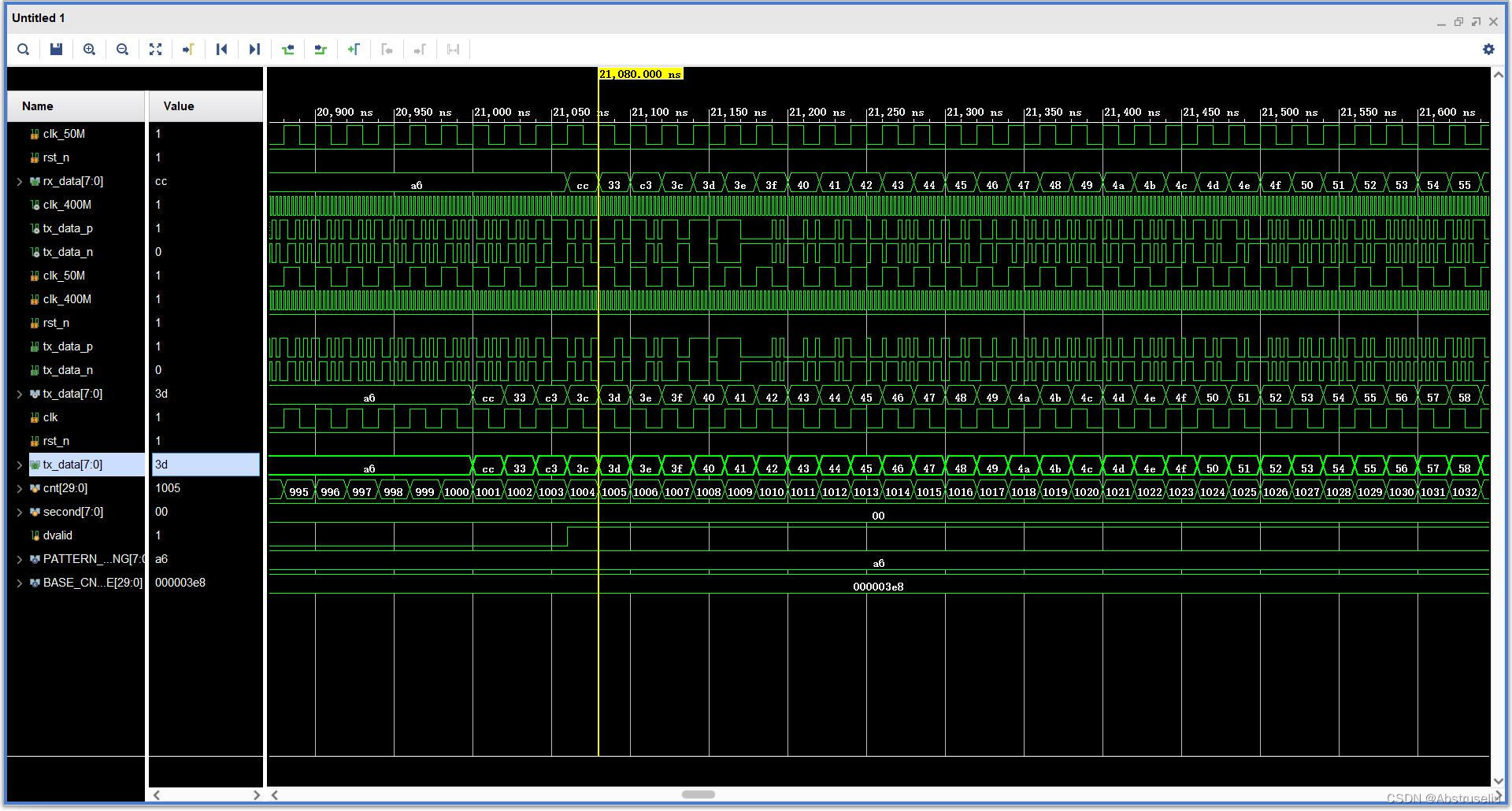
收获一:搭建LVDS数据环回工程功能仿真通过。
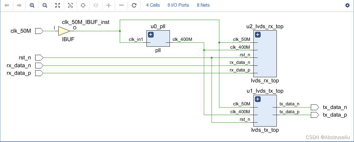
Ps.1:差分信号两根线但I/O Planning里只能分配p端引脚,因为p/n是一一对应的关系,分配的p端引脚其n端必须与原理图对应。
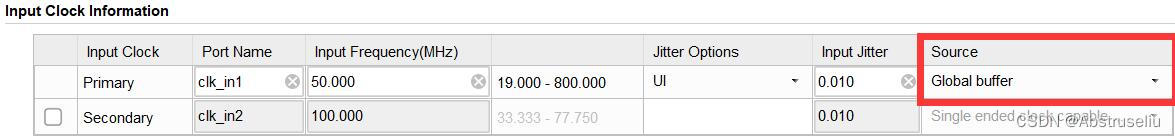
 Ps.2:设计实现时报错([DRC REQP-1712] Input clock driver: Unsupported PLLE2_ADV connectivity. The signal u0_pll/inst/clk_in1 on the u0_pll/inst/plle2_adv_inst/CLKIN1 pin of u0_pll/inst/plle2_adv_inst with COMPENSATION mode ZHOLD must be driven by a clock capable IO.) ,将锁相环IP中输入时钟源设置为Global buffer即可解决。 Ps.2:设计实现时报错([DRC REQP-1712] Input clock driver: Unsupported PLLE2_ADV connectivity. The signal u0_pll/inst/clk_in1 on the u0_pll/inst/plle2_adv_inst/CLKIN1 pin of u0_pll/inst/plle2_adv_inst with COMPENSATION mode ZHOLD must be driven by a clock capable IO.) ,将锁相环IP中输入时钟源设置为Global buffer即可解决。
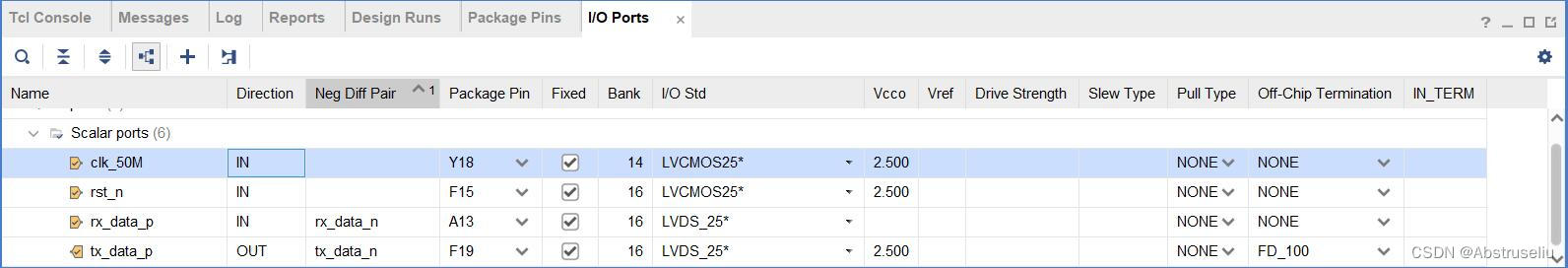
 Ps.3:设计实现时报错([DRC BIVC-1] Bank IO standard Vcc: Conflicting Vcc voltages in bank 16. For example, the following two ports in this bank have conflicting VCCOs: rst_n (LVCMOS33, requiring VCCO=3.300) and tx_data_p (LVDS_25, requiring VCCO=2.500) ),FPGA为了同时能和多种不同的电平标准接口芯片通信,Vcco通常以BANK为界,互相之间相互独立,也就是说在一颗FPGA芯片上同时存在几种不同的I/O电压。当然同一个BANK只能存在1种I/O电压。 Ps.3:设计实现时报错([DRC BIVC-1] Bank IO standard Vcc: Conflicting Vcc voltages in bank 16. For example, the following two ports in this bank have conflicting VCCOs: rst_n (LVCMOS33, requiring VCCO=3.300) and tx_data_p (LVDS_25, requiring VCCO=2.500) ),FPGA为了同时能和多种不同的电平标准接口芯片通信,Vcco通常以BANK为界,互相之间相互独立,也就是说在一颗FPGA芯片上同时存在几种不同的I/O电压。当然同一个BANK只能存在1种I/O电压。
|