关于栅极驱动器自举电路的考虑 |
您所在的位置:网站首页 › 栅极驱动器电流 › 关于栅极驱动器自举电路的考虑 |
关于栅极驱动器自举电路的考虑
|
介绍Driving a half-bridge based on N-channel MOSFETs or IGBTs requires providing to the high-side switch a gate voltage greater than the main supply. Without this overdrive, the high-side switch is not properly biased, and the power stage performance is heavily impacted. 驱动基于N沟道MOSFET或IGBT的半桥需要向高侧开关提供比主电源更大的栅极电压。如果没有这种过驱动,高端开关就不会被适当偏置,功率级性能也会受到严重影响。 One of the most common methods to generate this extra voltage is a bootstrap circuitry composed by a capacitor and diode series connected to the switching node.产生这种额外电压的最常见方法之一是由电容器和二极管组成的自举电路串联连接到交换节点。 This document describes the basic principles of this circuitry and provide guidelines on the proper selection of the components.本文件描述了该电路的基本原理,并提供了正确选择部件的指南。 基本原理自举电路的典型示意图如图1所示。 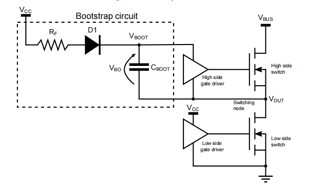 图1.自举电路图 图1.自举电路图当LS开关接通时,CBOOT自举电容器通过自举二极管(D1)充电。转弯在HS开关上,OUT节点上升到VBUS并且二极管被反向偏置。CBOOT(VBO)上的电压为因此VBOOT上升到VBUS以上以提供保持HS所需的额外电压。 When the LS switch is on, the CBOOT bootstrap capacitor is charged through the bootstrap diode (D1). Turning on the HS switch, the OUT node rises to VBUS and diode is reverse biased. The voltage on CBOOT (VBO) is maintained, consequently VBOOT rises above VBUS providing the extra-voltage needed for keeping on the HS.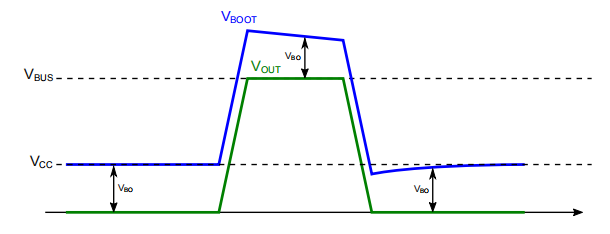 图2.时序图充电和放电阶段 图2.时序图充电和放电阶段如前一节所述,自举电容器的充电是强制将OUT节点通过LS开关。 Charge and discharge phases As introduced in the previous section, the charge of the bootstrap capacitor is performed forcing to ground the OUT node through the LS switch.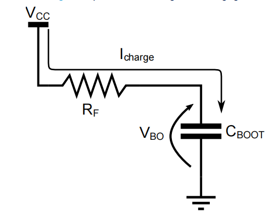 图3.CBOOT充电期间的等效电路 图3.CBOOT充电期间的等效电路在充电阶段,自举电容器上的电压增加由以下公式描述: 方程式1 V_{BO}(t)= (V_{CC}− V_{F})+ (V_{BO}( t0)− (V_{CC} − V_{F}) )∙ e^{\frac{−t}{R_{F} ∙ C_{BOOT}}} \\ 其中: •VBO是自举电容器CBOOT上的电压 •VBO(t0)是充电阶段开始时的启动电压 •VCC是栅极驱动器电源电压 •VF是自举二极管的正向电压(图1中的D1) •RF是自举电路的等效串联电阻,包括自举的导通电阻二极管(图1中的D1)。 当HS接通时,自举电容器放电 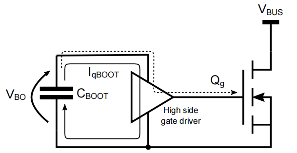 图4.CBOOT放电时的等效电路 图4.CBOOT放电时的等效电路在这种情况下,使用提供给驱动电路的电荷来计算VBO变化更为方便。由两部分组成:HS门驱动电路提供的一部分,用于打开开关(即总门电荷)和保持电路偏置所需的一个。 In this case it is more convenient to calculate the VBO variation using the charge provided to the driving circuitry. Composed by two parts: the one provided by the HS gate driving circuitry to turn on the switch (i.e. the Total Gate Charge) and the one needed to keep the circuitry biased.得出的公式为: 方程式2 \Delta V_{BO}(t)=\frac{Q_{g}+I_{BOOTq}\times t}{C_{BOOT}} \\ 其中: •ΔVBO是放电阶段的电压降低 •Qg是HS的总栅极电荷 •IBOOTq是连接到CBOOT的电路的静态电流。 使用等式2来计算等式1的VBO(t0),可以估计在每个充电和放电循环结束。在下面的部分中,描述了一些常见的用例。 恒定工作循环在开关频率和占空比恒定的情况下,HS和LS开关的接通时间为也是恒定的。在大约5倍于RF∙CBOOT的稳定时间之后,自举过驱动电压随着电荷而稳定电压变化等于放电变化。从方程1和方程2开始,最小电压(即在放电阶段结束时)可以是使用以下公式计算: 
|
【本文地址】