GD32的flash读保护和写保护 |
您所在的位置:网站首页 › 怎么去除写保护模式 › GD32的flash读保护和写保护 |
GD32的flash读保护和写保护
|
介绍
在实际发布的产品中,在GD32芯片的内部FLASH存储了控制程序,如果不作任何保护措施的话,可以使用下载器直接把内部FLASH的内容读取回来,得到bin或hex文件格式的代码拷贝,别有用心的厂商会利用该方法山寨产品。为此,GD32芯片提供了多种方式保护内部FLASH的程序不被非法读取,但在默认情况”下该保护功能是不开启的,若要开启该功能,需要改写内部FLASH选项字节(Option Bytes)中的配置。 GD32的选项字节地址和功能都跟STM32一样: 和flash一样,对选项字节进行擦除和编程都需要先解锁。 ob_unlock(); ob_lock(); 选项字节擦除函数 /* erase all the option Bytes */ fmc_state = ob_erase(); 选项字节编程函数FMC提供了一个32位整字/16位半字编程功能,可用来修改可选字节块内容。可选字节块共有8对可选字节。每对可选字节的高字节是低字节的补。当低字节被修改时,FMC自动生成该选项字节的高字节。 需要注意的是,执行整字/半字编程操作需要检查目的地址是否已经被擦除。 如果该地址没有被擦除, 对该地址写一个非0x0值, FMC_STAT0寄存器的PGERR位将被置1,对该地址的编程操作无效(当写内容为0x0时,即使目的地址没有被 正常擦除,也可以正确编程)。 当可选字节被改变时,需要系统复位使之生效。 使能写保护 /*! \brief enable write protection \param[in] ob_wp: specify sector to be write protected, set the bit to 1 if you want to protect the corresponding pages. meanwhile, sector macro could used to set specific sector write protected. one or more parameters can be selected which are shown as below: \arg OB_WPx(x = 0..31): write protect specify sector \arg OB_WP_ALL: write protect all sector \param[out] none \retval state of FMC, refer to fmc_state_enum */ fmc_state_enum ob_write_protection_enable(uint32_t ob_wp)选项字节的WP[30:0]中的每个bit设置每4KB flash空间的保护状态,比如最低位设置最开始4KB空间的写保护状态,即0x0800 0000 - 0x0800 0FFF。这31位总计可设置前124KB的闪存保护状态。 WP[31],第31位可设置闪存剩下部分的保护状态。 库函数都已经把每个扇区的宏定义写好了: /* option bytes write protection */ #define OB_WP_0 ((uint32_t)0x00000001U) /*!< erase/program protection of sector 0 */ #define OB_WP_1 ((uint32_t)0x00000002U) /*!< erase/program protection of sector 1 */ #define OB_WP_2 ((uint32_t)0x00000004U) /*!< erase/program protection of sector 2 */ #define OB_WP_3 ((uint32_t)0x00000008U) /*!< erase/program protection of sector 3 */ #define OB_WP_4 ((uint32_t)0x00000010U) /*!< erase/program protection of sector 4 */ #define OB_WP_5 ((uint32_t)0x00000020U) /*!< erase/program protection of sector 5 */ #define OB_WP_6 ((uint32_t)0x00000040U) /*!< erase/program protection of sector 6 */ #define OB_WP_7 ((uint32_t)0x00000080U) /*!< erase/program protection of sector 7 */ #define OB_WP_8 ((uint32_t)0x00000100U) /*!< erase/program protection of sector 8 */ #define OB_WP_9 ((uint32_t)0x00000200U) /*!< erase/program protection of sector 9 */ #define OB_WP_10 ((uint32_t)0x00000400U) /*!< erase/program protection of sector 10 */ #define OB_WP_11 ((uint32_t)0x00000800U) /*!< erase/program protection of sector 11 */ #define OB_WP_12 ((uint32_t)0x00001000U) /*!< erase/program protection of sector 12 */ #define OB_WP_13 ((uint32_t)0x00002000U) /*!< erase/program protection of sector 13 */ #define OB_WP_14 ((uint32_t)0x00004000U) /*!< erase/program protection of sector 14 */ #define OB_WP_15 ((uint32_t)0x00008000U) /*!< erase/program protection of sector 15 */ #define OB_WP_16 ((uint32_t)0x00010000U) /*!< erase/program protection of sector 16 */ #define OB_WP_17 ((uint32_t)0x00020000U) /*!< erase/program protection of sector 17 */ #define OB_WP_18 ((uint32_t)0x00040000U) /*!< erase/program protection of sector 18 */ #define OB_WP_19 ((uint32_t)0x00080000U) /*!< erase/program protection of sector 19 */ #define OB_WP_20 ((uint32_t)0x00100000U) /*!< erase/program protection of sector 20 */ #define OB_WP_21 ((uint32_t)0x00200000U) /*!< erase/program protection of sector 21 */ #define OB_WP_22 ((uint32_t)0x00400000U) /*!< erase/program protection of sector 22 */ #define OB_WP_23 ((uint32_t)0x00800000U) /*!< erase/program protection of sector 23 */ #define OB_WP_24 ((uint32_t)0x01000000U) /*!< erase/program protection of sector 24 */ #define OB_WP_25 ((uint32_t)0x02000000U) /*!< erase/program protection of sector 25 */ #define OB_WP_26 ((uint32_t)0x04000000U) /*!< erase/program protection of sector 26 */ #define OB_WP_27 ((uint32_t)0x08000000U) /*!< erase/program protection of sector 27 */ #define OB_WP_28 ((uint32_t)0x10000000U) /*!< erase/program protection of sector 28 */ #define OB_WP_29 ((uint32_t)0x20000000U) /*!< erase/program protection of sector 29 */ #define OB_WP_30 ((uint32_t)0x40000000U) /*!< erase/program protection of sector 30 */ #define OB_WP_31 ((uint32_t)0x80000000U) /*!< erase/program protection of sector 31 */ #define OB_WP_ALL ((uint32_t)0xFFFFFFFFU) /*!< erase/program protection of all sectors */比如,要写保护扇区0,执行: ob_write_protection_enable(OB_WP_0);要写保护扇区0、1、2,执行: ob_write_protection_enable(OB_WP_0|OB_WP_1|OB_WP_2); 使能读保护FMC提供了一个安全保护功能来阻止非法读取闪存。 此功能可以很好地保护软件和固件免受非法的用户操作。 未保护状态:当将SPC字节和它的补字节被设置为0x5AA5,系统复位以后,闪存将处于非安全保护状态。主存储块和可选字节块可以被所有操作模式访问。 已保护状态:当设置SPC字节和它的补字节值为任何除0x5AA5外的值,系统复位以后,安全保护状态生效。需要注意的是, 若该修改过程中,MCU的调试模块依然和外部JTAG/SWD设备相连,需要用上电复位代替系统复位以使得修改后的保护状态生效。在安全保护状态下,主存储闪存块仅能被用户代码访问且前4KB的闪存自动处于页擦除/编程保护状态下。 在调试模式下,或从SRAM中启动时,以及从boot loader区启动时,这些模式下对主存储块的操作都被禁止。如果在这些模式下读主存储块,将产生总线错误。如果在这些模式下,对主存储块进行编程或擦除操作, FMC_STAT寄存器的WPERR位将被置1。 但这些模式下都可以对可选字节块进行操作,从而可以通过该方式失能安全保护功能。如果将SPC字节和它的补字节设置为0x5AA5,安全保护功能将失效,并自动触发一次整片擦除操作。 /*! \brief configure security protection \param[in] ob_spc: specify security protection only one parameter can be selected which is shown as below: \arg FMC_NSPC: no security protection \arg FMC_USPC: under security protection \param[out] none \retval state of FMC, refer to fmc_state_enum */ fmc_state_enum ob_security_protection_config(uint8_t ob_spc)要使能读保护,执行 ob_security_protection_config(FMC_USPC);要取消读保护,执行 ob_security_protection_config(FMC_NSPC); |
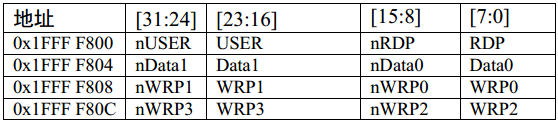 其中前面带“n”的是不带“n”的取反,即nUSER的值等于(~USER)、nRDP的值等于(~RDP),GD32利用反码来确保选项字节内容的正确性。 每次系统复位后,闪存的可选字节块被重加载到FMC_OBSTAT和FMC_WP寄存器,可选字节生效。可选字节的补字节具体为可选字节取反。当可选字节被重装载时,如果可选字节的补字节和可选字节不匹配,FMC_OBSTAT寄存器的OBERR位将被置1,可选字节被强制设置为0xFF。若可选字节和其补字节同为0xFF,则OBERR位不置位。可选字节详情见下表。
【本文地址】
今日新闻 |
推荐新闻 |