nodeMCU |
您所在的位置:网站首页 › sn74ls123n引脚图 › nodeMCU |
nodeMCU
|
文章目录
reference material通讯NodeMCU Development Board Pinout Configuration特殊引脚情况说明🤣🤷♂️建议查阅NodeMCU datasheetBest Pins to Use – ESP8266GPIO0(D3)GPIO2(D4)GPIO15(D8)
Esp8266芯片的模拟输入
串行端口I²CSPIESP8266引脚功能一览
来自谷歌图片
reference material
esp8266 datasheet:NodeMCU ESP8266 Pinout, Specifications, Features & Datasheet (components101.com)NodeMCU开发板详解 (第1章-第2节) – 太极创客 (taichi-maker.com)ESP8266 Pinout Reference: Which GPIO pins should you use? | Random Nerd Tutorials
通讯
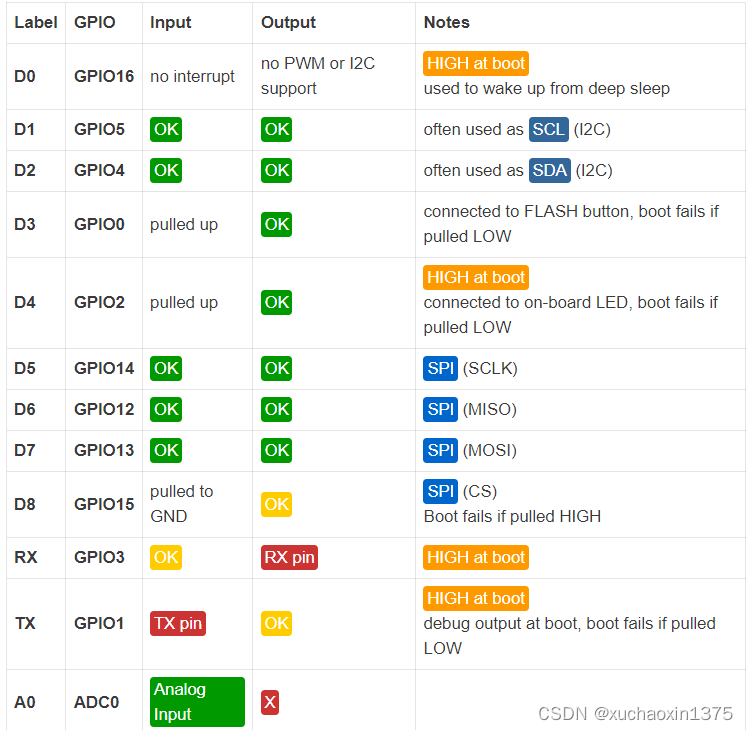
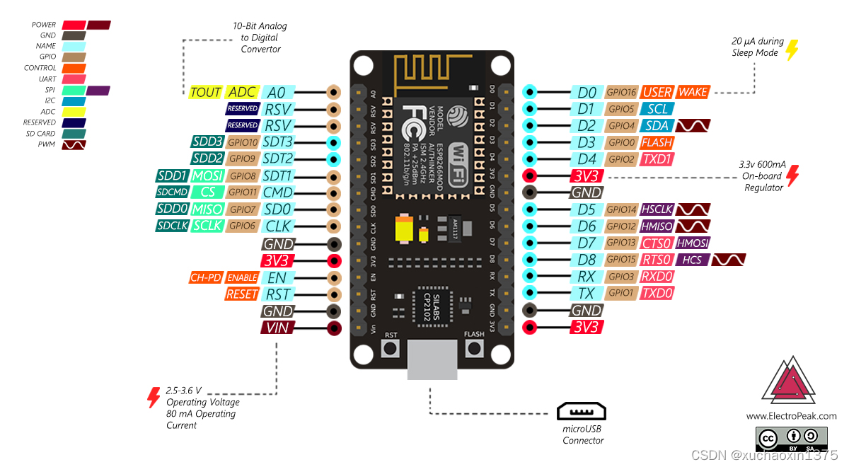
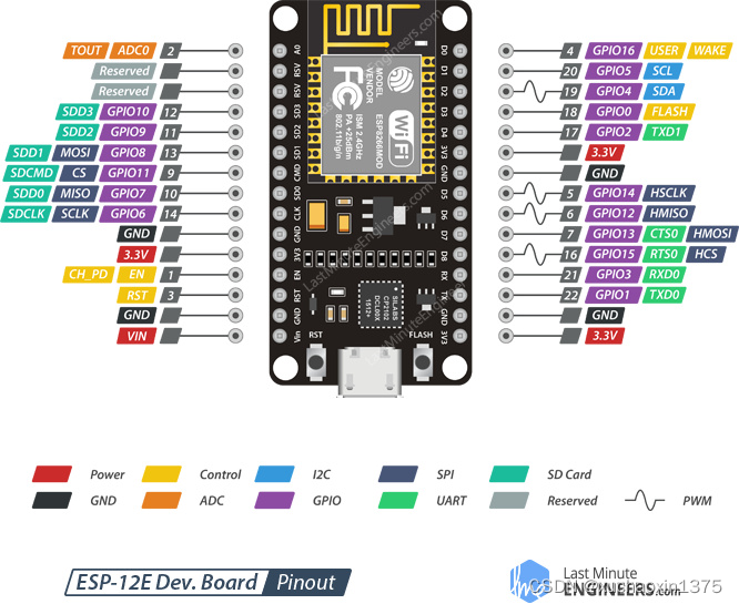
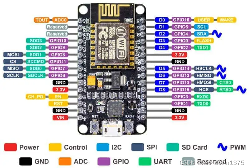
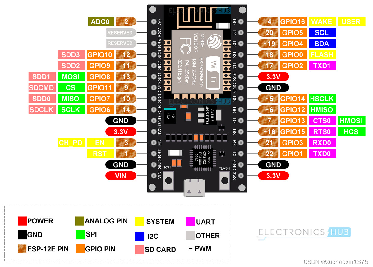
NodeMCU is an open-source Lua based firmware and development board specially targeted for IoT based Applications. It includes firmware that runs on the ESP8266 Wi-Fi SoC from Espressif Systems, and hardware which is based on the ESP-12 module. NodeMCU Development Board Pinout Configuration Pin CategoryNameDescriptionPowerMicro-USB, 3.3V, GND, VinMicro-USB: NodeMCU can be powered through the USB port 3.3V: Regulated 3.3V can be supplied to this pin to power the board GND: Ground pins Vin: External Power SupplyControl PinsEN, RSTThe pin and the button resets the microcontrollerAnalog PinA0Used to measure analog voltage in the range of 0-3.3VGPIO PinsGPIO1 to GPIO16NodeMCU has 16 general purpose input-output pins on its boardSPI PinsSD1, CMD, SD0, CLKNodeMCU has four pins available for SPI communication.UART PinsTXD0, RXD0, TXD2, RXD2NodeMCU has two UART interfaces, UART0 (RXD0 & TXD0) and UART1 (RXD1 & TXD1). UART1 is used to upload the firmware/program.I2C PinsNodeMCU has I2C functionality support but due to the internal functionality of these pins, you have to find which pin is I2C. 特殊引脚情况说明🤣🤷♂️ 建议查阅NodeMCU datasheet 以下内容为第三方描述,可能存在不准确性参考连接: NodeMCU ESP8266 GPIO 和 PWM 学习 | 匠心博客 (zhaomenghuan.js.org)Nodemcu的GPIO接口介绍 – 八色木 (basemu.com) Best Pins to Use – ESP8266One important thing to notice about ESP8266 is that the GPIO number doesn’t match the label on the board silkscreen. For example, D0 corresponds to GPIO16 and D1 corresponds to GPIO5. The following table shows the correspondence between the labels on the silkscreen and the GPIO number as well as what pins are the best to use in your projects, and which ones you need to be cautious. The pins highlighted in green are OK to use. The ones highlighted in yellow are OK to use, but you need to pay attention because they may have unexpected behavior mainly at boot. The pins highlighted in red are not recommended to use as inputs or outputs. 您无需对GPIO0引脚进行额外操作,因为NodeMCU的内置电路可以确保GPIO0引脚在工作时连接高电平而在上传程序时连接低电平。 GPIO2(D4) GPIO2(D4)引脚在NodeMCU开发板启动时是不能连接低电平的。 实际使用过程中,D4电平不向其他管脚可以被拉低到和GND一样低,也就是说,该引脚不太推荐使用,容易掉坑;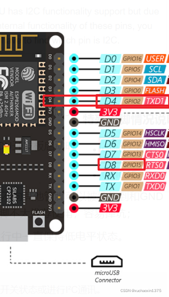 GPIO15(D8)
引脚在开发板运行中一直保持低电平状态。
GPIO15(D8)
GPIO15(D8)引脚在开发板运行中一直保持低电平状态。
因此请不要使用GPIO15引脚来读取开关状态或进行I²C通讯。 上拉电阻/下拉电阻 GPIO 0-15引脚都配有内置上拉电阻。这一点与Arduino十分类似。GPIO16 引脚配有内置下拉电阻。 Esp8266芯片的模拟输入 ESP8266 只有一个模拟输入引脚(该引脚通过模拟-数字转换将引脚上的模拟电压数值转化为数字量)。此引脚可以读取的模拟电压值为 0 – 1.0V。请注意:ESP8266 芯片模拟输入引脚连接在1.0V以上电压可能损坏ESP8266芯片。以上所描述的是针对ESP8266芯片的引脚。 幸运的是,对于NodeMCU开发板引脚,情况就不同了。 NodeMCU开发板配有降压电路。您可以用NodeMCU开发板的模拟输入引脚读取0-3.3V的模拟电压信号。 串行端口ESP8266有2个硬件串行端口(UART)。 串行端口0(UART0)使用GPIO1和GPIO3引脚。其中GPIO1引脚是TX0,GPIO3是RX0。 串行端口1(UART1)使用GPIO2和GPIO8引脚。其中GPIO2引脚是TX1,GPIO8是RX1。请注意,由于GPIO8被用于连接闪存芯片,串行端口1只能使用GPIO2来向外发送串行数据。 I²CESP8266只有软件模拟的I²C端口,没有硬件I²C端口。也就是说我们可以使用任意的两个GPIO引脚通过软件模拟来实现I²C通讯。ESP8266的数据表(datasheet)中,GPIO2标注为SDA,GPIO14标注为SCL。 SPIESP8266的SPI端口情况如下: GPIO14 — CLK GPIO12 — MISO GPIO13 — MOSI GPIO 15 — CS(SS) ESP8266引脚功能一览 GPIO功能状态限制0引导模式选择3.3V无Hi-Z1TX0–串口通讯过程中不能使用2引导模式选择 TX13.3V启动时不能接地 启动时发送调试信息3RX0–串口通讯过程中不能使用4SDA (I²C)––5SCL (I²C)––6 – 11连接闪存x不可用12MISO (SPI)––13MOSI (SPI)––14SCK (SPI)––15SS (SPI)0V上拉电阻不可用16睡眠唤醒–无上拉电阻,仅有下拉电阻 连接 RST 引脚实现睡眠唤醒 来自谷歌图片
|
 SD系列的不建议使用
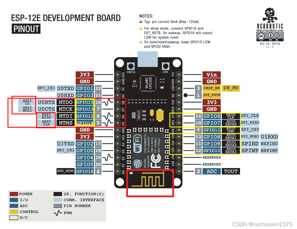
【本文地址】
今日新闻 |
推荐新闻 |