OPAMP可选增益运算放大器(电路原理及应用) |
您所在的位置:网站首页 › pa05运算放大器 › OPAMP可选增益运算放大器(电路原理及应用) |
OPAMP可选增益运算放大器(电路原理及应用)
|
文章目录
工作原理放大倍率电路设计说明应用电路
OPAMP+ADC的应用
工作原理
放大倍率
 b. 在相电流为零的条件下,选择合适的参数使Vin经放大后的电压Vout为MCU供电电压的一半(V_m/2),从而尽可能的利用ADC的采集范围[0,ADC_Vsupply],一般使采集值覆盖85-90%的范围 c.
V
i
n
V_{in}
Vin与采样电阻电压关系:
V
i
n
+
=
R
2
∗
R
3
R
2
∗
R
3
+
R
1
∗
R
3
+
R
1
∗
R
2
V
s
h
u
n
t
V_{in}+ = \frac{R_2*R_3}{R_2*R_3+R_1*R_3+R_1*R_2}V_{shunt}
Vin+=R2∗R3+R1∗R3+R1∗R2R2∗R3Vshunt
上式中:流过采样电阻RShunt的电流约等于相电流,经R1到RShunt的电流忽略不计 d. 放大器的特性使得Vin+ = Vin-R4和R5 U1A构成放大电路,其产生的增益G2与G1一起构成总的增益G
V
o
p
a
m
p
_
o
u
t
=
(
1
+
R
5
R
4
)
∗
V
i
n
+
V_{opamp\_out} = (1+\frac{R_5}{R_4})*V_{in}+
Vopamp_out=(1+R4R5)∗Vin+
电路设计说明
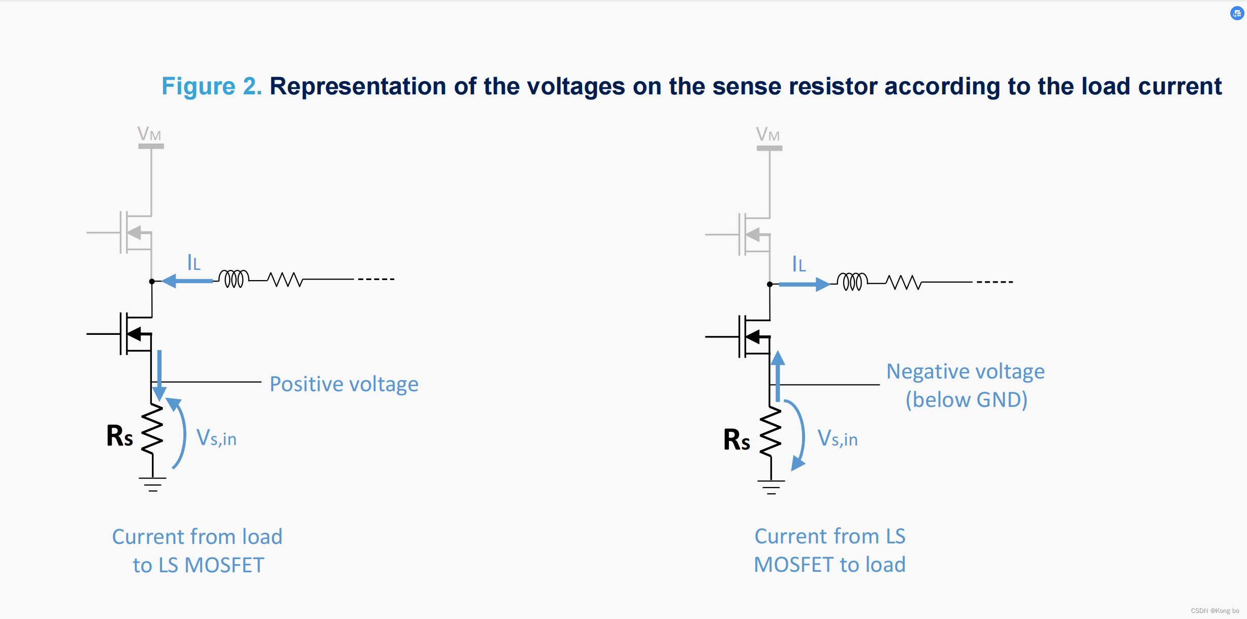
以下是ST对该采样电路在设计上的说明,可在官网st.com搜索AN5397找到该文档,简单的来说就是通过差分来消除地线信号的干扰(运放的虚短特性使
V
i
n
+
V_{in}+
Vin+=
V
i
n
−
V_{in}-
Vin−,从而使干扰信号在输入端的影响相同而抵消) AN5397 The schematic of the improved solution is represented in Figure 8. The signal coming from the sense resistor is acquired as a differential signal. The ground reference is split between the power GND, which the sense resistor is referred to, and the signal GND, which is the reference for the amplified signal and the ADC. In fact, when high currents flow through the GND path, a common mode voltage is generated on the sense resistor, due to parasitic inductances distributed on the path (see Figure 9). If not rejected, the common mode voltage is amplified as a signal and it can introduce an error. The differential configuration depicted in Figure 8 allows to overcome this issue. As shown in Figure 8, the different GND paths must be kept separated and connected together just in one point of the PCB, usually the GND of the main power supply. Moreover, the two traces coming from the sense resistor must be treated as differential traces: they are connected as close as possible to the sense resistor terminals and run symmetrically and side by side towards the op-amp. b. 在相电流为零的条件下,选择合适的参数使Vin经放大后的电压Vout为MCU供电电压的一半(V_m/2),从而尽可能的利用ADC的采集范围[0,ADC_Vsupply],一般使采集值覆盖85-90%的范围 c.
V
i
n
V_{in}
Vin与采样电阻电压关系:
V
i
n
+
=
R
2
∗
R
3
R
2
∗
R
3
+
R
1
∗
R
3
+
R
1
∗
R
2
V
s
h
u
n
t
V_{in}+ = \frac{R_2*R_3}{R_2*R_3+R_1*R_3+R_1*R_2}V_{shunt}
Vin+=R2∗R3+R1∗R3+R1∗R2R2∗R3Vshunt
上式中:流过采样电阻RShunt的电流约等于相电流,经R1到RShunt的电流忽略不计 d. 放大器的特性使得Vin+ = Vin-R4和R5 U1A构成放大电路,其产生的增益G2与G1一起构成总的增益G
V
o
p
a
m
p
_
o
u
t
=
(
1
+
R
5
R
4
)
∗
V
i
n
+
V_{opamp\_out} = (1+\frac{R_5}{R_4})*V_{in}+
Vopamp_out=(1+R4R5)∗Vin+
电路设计说明
以下是ST对该采样电路在设计上的说明,可在官网st.com搜索AN5397找到该文档,简单的来说就是通过差分来消除地线信号的干扰(运放的虚短特性使
V
i
n
+
V_{in}+
Vin+=
V
i
n
−
V_{in}-
Vin−,从而使干扰信号在输入端的影响相同而抵消) AN5397 The schematic of the improved solution is represented in Figure 8. The signal coming from the sense resistor is acquired as a differential signal. The ground reference is split between the power GND, which the sense resistor is referred to, and the signal GND, which is the reference for the amplified signal and the ADC. In fact, when high currents flow through the GND path, a common mode voltage is generated on the sense resistor, due to parasitic inductances distributed on the path (see Figure 9). If not rejected, the common mode voltage is amplified as a signal and it can introduce an error. The differential configuration depicted in Figure 8 allows to overcome this issue. As shown in Figure 8, the different GND paths must be kept separated and connected together just in one point of the PCB, usually the GND of the main power supply. Moreover, the two traces coming from the sense resistor must be treated as differential traces: they are connected as close as possible to the sense resistor terminals and run symmetrically and side by side towards the op-amp.   OPAMP通过调节内部电阻实现对放大倍率的控制 OPAMP通过调节内部电阻实现对放大倍率的控制  STM32G431的OPAMP可选的放大倍率最大为64,即
V
o
p
a
m
p
_
o
u
t
=
64
V
i
n
V_{opamp\_out} = 64V_{in}
Vopamp_out=64Vin STM32G431的OPAMP可选的放大倍率最大为64,即
V
o
p
a
m
p
_
o
u
t
=
64
V
i
n
V_{opamp\_out} = 64V_{in}
Vopamp_out=64Vin  Example Example  应用电路
应用电路
Vshunt_x-接到采样电阻的负端(GND) 将引脚设置为如下模式
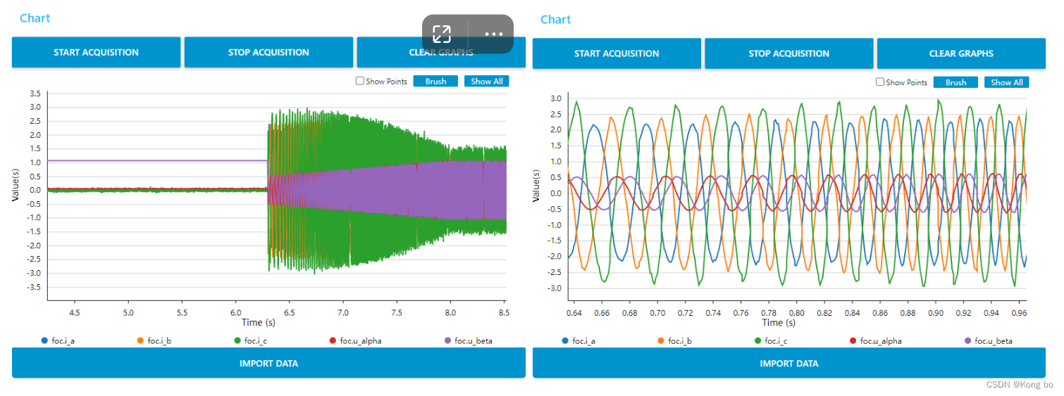
注:CubeMonitor最大采样率为1KHz,所以曲线并不光滑 使用ADC中断 读数据 adc_injected_buffer[0] = hadc1.Instance->JDR1 * 3.3 / 4096; adc_injected_buffer[1] = hadc1.Instance->JDR2 * 3.3 / 4096; adc_injected_buffer[2] = hadc2.Instance->JDR1 * 3.3 / 4096;ADC的中断回调函数 void HAL_ADC_ConvCpltCallback(ADC_HandleTypeDef* hadc) |


 使能OPAMP为如下模式并设置PGA增益
  ADC1的配置如下,我们使用ADC的Injected模式对OPAMP的输出进行采样,ADC2同理
  注意:如果是对电机相电流进行ADC采样,要在上桥臂关断下桥臂导通时进行采样,在MOS开关时有较大扰动,具体内容会在后面的推文中进行实验讲解
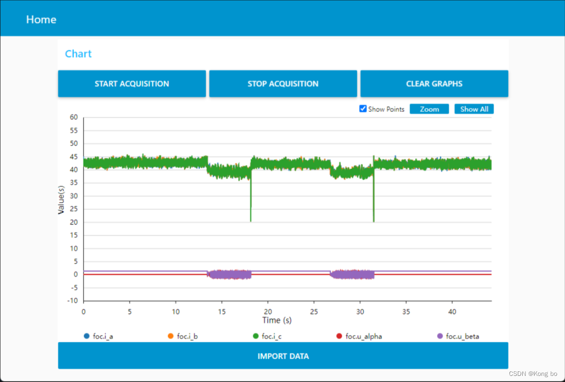
 初始化
初始化【本文地址】